
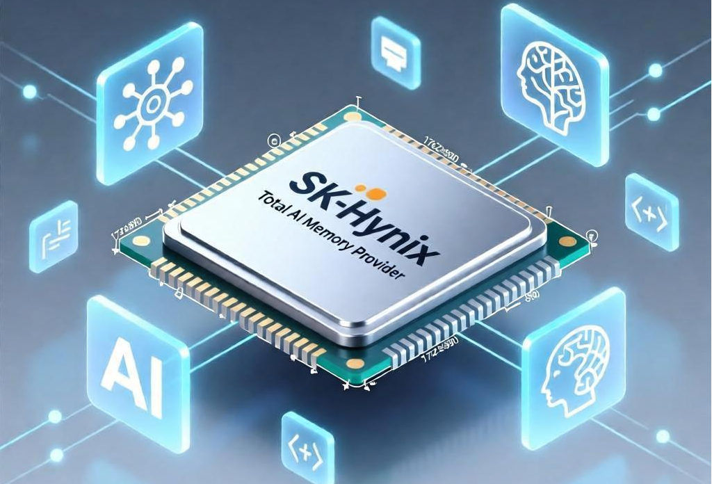
SK hynix is moving beyond its roots as a commodity chipmaker. With its new “Total AI Memory Provider” strategy, the company is pivoting from selling passive, standardized parts to developing “active” memory that is deeply integrated into the AI silicon stack.
The blueprint for this transformation follows a three-step offensive:
The Custom HBM Era: Beginning with HBM4E in 2026, SK hynix will integrate controllers and even logic functions directly into the HBM base die. By blurring the line between memory and processors, they aim to slash data latency and power consumption—a move that has already drawn interest from titans like NVIDIA and Apple.
Reinventing DRAM: Through its AI-D initiative, the company is scaling bandwidth with MRDIMM technology while exploring “Processing-In-Memory” (PIM) and CXL to finally break the “memory wall.” The goal is to move DRAM beyond the data center and into the edge, powering next-gen robotics and mobile AI.
High-Bandwidth NAND: By 2027, the company plans to debut High Bandwidth Flash (HBF), a hybrid tech that marries HBM-like speeds with NAND’s massive density. Combined with 400-layer stacking, this creates a path toward PB-level storage optimized specifically for AI inference.
As Samsung and Micron ramp up their own efforts, SK hynix’s “secret weapon” is clear: memory is no longer just a warehouse for data—it’s becoming a co-processor in the AI engin
